Posts Tagged ‘SMT’
 Summer SMT Project
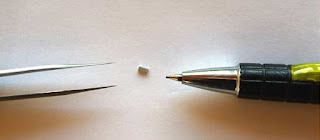
Over the past week, I've been playing with my 630m transverter summer project.
It's not the normal type of transverter that would produce a signal on 630m (~475kHz) but rather, one that will produce a signal on twice this frequency. My630m amplifier, using switching FETs, was designed and built with a 'divide-by-two' input circuit, to allow for greater frequency resolution when first constructed as a 2200m system. I really don't want to modify the transmitter and prefer just to be able to unplug my DDS and plug-in the transverter, allowing me to run WSPR, JT9 and several other digital modes when needed.
So far I've not been able to get the transverter to produce the desired low voltage 950kHz squarewave output, although I'm closer than when I began the troubleshooting.
My circuit is basically a G3XBM 630m transverter, without the FET final amplifier. Instead, the driver feeds a full-wave rectifier frequency doubler for 630m, designed and published a few years ago by Jay, W1VD. Although I can get a squarewave end result, I think harmonics creeping into the process earlier down the mixing chain are causing non-symmetry in the output.
 |
| 3.2MHz signal out of oscillator buffer stage |
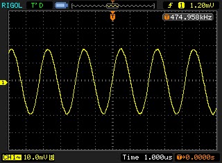 | |||
| 475 kHz signal out of mixer stage |
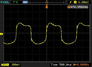 |
| Signal out of 'squarer' stage |
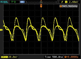 |
| Signal out of full-wave bridge |
 |
| Signal out of LPF |
 |
| Asymmetrical squarewave from 4046 output |
I've tried a 3-section LPF with a cutoff of ~600kHz between the mixer output and the next stage, trying to knock down the 'sum' frequency of 6.875MHz and any crystal harmonics but have since replaced this with a 630m diplexer at the mixer output to pass anything below 1MHz to the squarer and anything above 1.5MHz to ground. I'll keep playing with it ... until it works as it should or I have no hair left to pull out. I may also just rebuild the circuit, Manhattan-style, with normal sized parts, making it much easier to change or modify as I need. The scope grabs shown above are with the diplexer in place at the mixer output. It seems like something in the full-wave frequency doubler is amiss. I've looked at T1, the bifilar transformer several times but don't see anything odd but that's the stage where things seem to go south. Maybe it's an impedance matching-thing, something I'm yet uncomfortable with when it comes to properly matching various stages.
I also now realize that the section of transverter I have chosen will require post-mixer filtering, not shown in the schematic. Not using the last stage (FET PA) and its associated filtering, has no doubt caused more harmonics to appear in the output than anticipated. If I redesign and rebuild, I will add an LPF after the crystal oscillator as well as at the RF input port and pay more attention to post-mixer filtering.
Another route to try, rather than the W1VD doubler, may be this 4069 IC doubler or a similar 4011 doubler.
Although the project outcomes have not yet been achieved, the process has been a positive one in a couple of respects and well worth the time spent so far.
I have learned that working with the 1206-sized SMT parts is much easier than suspected and in fact, populating the board with these tiny parts was a lot of fun. The 1206-sized parts are at the 'large' end of the SMT size-spectrum ... rest assured I won't be going any smaller, at least for now.
The other positive outcome was knowing that my PCB design process can work well with the narrower lines, pads and much smaller IC footprints. I still design my boards using MS Paint and have always been happy with the ease at which it works. I know many might scoff at MS Paint but it really is a very versatile little program, with a short learning curve, unlike many of the more sophisticated PCB design programs.
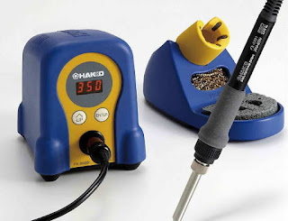
And one more positive outcome. I used the project as an excuse to purchase a new soldering station ... one that I had been lusting over for a few years as it is very SMT-friendly compared to my old Weller clunker. It also has an electrically isolated tip, unlike my Weller. The Hakko FX-888D turned out to be everything I had hoped and was no doubt part of the reason that I found the SMT process so enjoyable.
 |
| Add caption |
 630m Transverter Project
 I've ordered parts from Digikey for the summer workbench project, a 630m transverter. With the nice 630m WSPR signals received here from Roger (VK4YB) this spring, I think it might be possible for us to work each other using JT9, if the path continues to improve over the next few seasons. On more than one night, Roger's signal was at JT9 QSO levels and had we been on a schedule, a QSO may have happened. Roger's signal was peaking late in his evening, which for me will require making schedules in the wee hours of the morning.
I've been wanting to build another SMD project for some time since making a little SMK-1 40m transceiver several years ago. This was a very inexpensive kit put out by the NorCal QRP Club as a way of introducing SMD construction techniques to beginners. I found working with the 1206 sized parts (basically the largest ones commonly available) to be fairly laborious and would only solder a few parts at a time before setting it aside for the next day. I think my frustration had a lot to do with my positioning and soldering methods and I'm anxious to try doing it with a more refined technique. As I recall, there were 72 SMD components on the board and it took me a couple of weeks to finish it all.
 |
| My SMK-1 40m SMD transceiver |
The parts I have ordered are also 1206 sized but the older I get, the smaller these things seem to look. The transverter will be based partially on the popular G3XBM circuit but will eliminate the PA. Instead, I'll just use a few volts of the transverted squarewave signal and a doubler, so that I can feed the signal directly into my present homebrew amplifier which uses two switching FET modules into a power combiner. Hopefully this system will let me run several of the non-linear digital modes such as WSPR, JT9, JT65 etc.
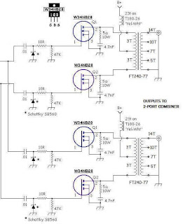 |
| My 630m PA |
As a way of getting back into the SMD-soldering groove, I have ordered and now received, an "SMD Practice Kit" from E-Bay ... a real bargain at $1.78!
 |
| courtesy: Tradeworld2105 |
Although there are many similar practice kits being offered on E-Bay, this was the only one I found that had two IC's to practice with ... all of the others had just one. Since the transverter's doubler circuit has an IC chip, a couple of practice opportunities will be helpful. My only hope is that I don't run out of SMD steam with the practice board before getting down to the actual transverter board.
As soon as the parts arrive from Digikey, I'll start designing the transverter's PCB ... but with all of the usual distractions of summer, as well as trying to maintain vigilance on the magic band once again, my summer project may not progress as quickly as I hope.
All of this assumes that my old eyeballs hold out as well.
 More SMT Talk
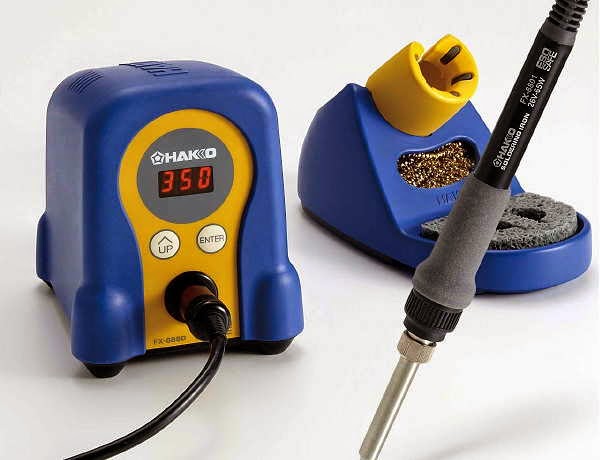 |
| Hakko FX-888D Soldering Station |
Jack was a NASA level B instructor for 26 years with Bristol Aerospace in Winnipeg, Manitoba. During that time he was instructing on an 'as required basis' but mainly working as an instructor and designer for the SCISAT-1 satellite. Worked involved all electrical systems, harnessing, manufacturing, designing of PC boards and all NASA hand-soldering and SMT soldering processes. That also included writing all the documentation for all the NASA processes used for the manufacturing and testing of the satellite electrical systems.
Although my first and only SMT experience several years ago resulted in the successful completion of a simple 40m transceiver, I found the process tedious and less than enjoyable. Jack suggested that my laborious technique was not the way to do it and was probably to blame for my negativity towards future SMT work. He gave me a wealth of encouraging suggestions for a more 'enjoyable' outcome:
Yes I agree our old eyes are not the same, but a good 6" magnifier ~2.25X lens with light (preferably incandescent IMHO), this is what I use plus a loop if needed for closer-up inspection. An alternate is a binocular magnifier with ~ 2.25X or better, they are widely used by inspectors, jewellers or home hobbyists.
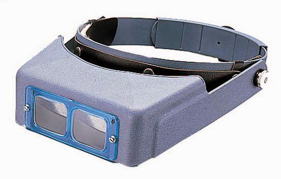 This is what I think I'll invest in next. Without these you haven't a hope or chance of doing the job as well, it is next to impossible. Sorry, not going to talk you out of building with SMT parts, We've gone from tubes to transistors and now to SMT, time to make the change :-)
 BTW, not sure what that instrument is that you have on the blog, looks something like a tool that may be used to hold down the chip while soldering. You don't need it.
Helpful hints if you so decide to go with SMT:
First purchase a good sharp pointed long ESD type plastic or metal tweezers.
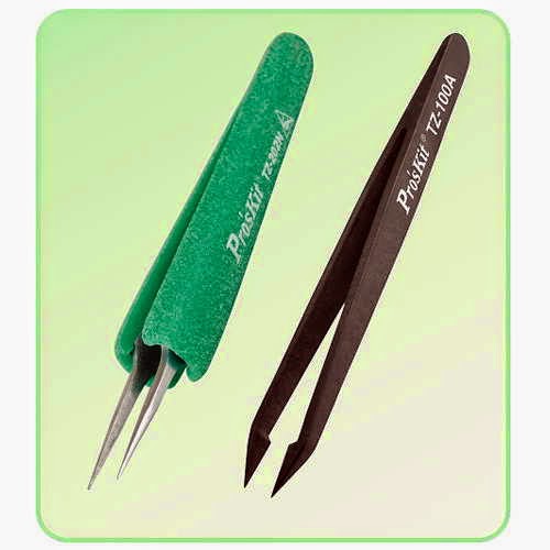
Tack solder one side only, then go to the other side of the chip and solder it correctly, THEN go back to the 1st side and re-solder that side correctly, keep your dwell time to <3-4 seconds. Start with using a tooth pick and apply a small drop of solder paste on each side of the chips pads. If soldering a large 14-16 pin chip, tack solder one corner then the opposite corner first being careful to have the correct alignment/position. Now apply solder paste down the length of each side, don't worry if you apply paste between the pads as the heat will draw it away once you apply the tip. Slowly draw the long soldering iron tip down each pad starting from any corner, allow a few seconds to cool, then repeat for the opposite side. Fine solder will also work but it's slow and far more time consuming.
Use liquid paste SN63/PB37 eutectic solder {no plastic state} for best application, use sparingly as it's too easy to get some under the chip which can easily cause a short cct.
Hope that helps you and convinces you to give it a try.
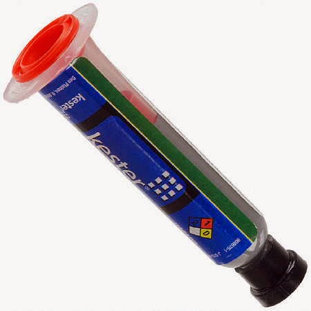 Personally, I prefer just 63/37 liquid paste in a syringe, far less cleaning up with IPA. Besides, using IPA means cleaning it 100% with a stiff bristle brush. Once the flux is exposed to IPA or rubbing alcohol, there is a chemical action that slowly takes place and it is quite corrosive if the area is not thoroughly washed. Besides, you can't afford to expose certain parts like pots that are not hermetically sealed, once the flux gets inside the pot is contaminated and becomes useless. It's OK to not clean your board, as long as you don't attempt to use any alcohol in a half-ass method. We used total immersion baths and not just one but three separate ones. Even then...I had to slowly pour pure distilled water over the board, capture it in a clean beaker then take it over to our chemical lab where they tested it for any flux residue. Those were required mainly for building all the satellite boards though. Most commercial manufacturers don't bother to clean their boards, a) one less manufacturing step, b) added cost and less chance of contamination. There are some no-clean solder pastes out there now, something to look into, see Digikey for examples. Don't worry about expiry date later down the road, mine expired in 2009! These paste manufacturers mainly deal with big companies that have a tight criteria to meet in order to comply with a wide range of standards imposed on them. Mine still works beautifully, I keep rotating it so the flux inside doesn't settle to just one side. Keeping it in a fridge can even extend the life, but don't worry about that, besides the xyl may not like the idea.
Yes, there have been many attempts back in the mid 70-80s to come up with a simple solution for a simple problem of having a third hand to hold the part in place while you hold the soldering iron with the other hand. NASA, ESA (European Space Agency) and IPC have never used anything like that since the very beginning. Although most hams probably wouldn't want to go to the trouble of learning NASA standards as it's a bit overkill, but it's far better than what some are portraying on the web as the right way to do it.
I'm not sure where that antiquated technique of using a large tool to hold down chips ever came from, but I'm guessing from hobbyists who meant well as they were not trained to know any other way. What hobbyists use for small work production are vacuum tools or what is referred to as "pick and place" machines or even simple ESD approved tweezers just to bring the part to the board. With solder paste already in place, the part is allowed to be placed onto its pads on top of the paste. The part is held with tweezers whilst the iron tip tacks one side for a couple of seconds then the tweezers can be removed, then the other side is heated. There is absolutely no need for a third hand. I see a lot of guys use regular small solder to do the soldering of SMT parts. Yes it can be used but it's awkward if you don't know what you are doing. Liquid rosin flux can also be used, a small bottle with a fine needle type end can be used to apply the rosin, followed by a small drop of solder on the end of the iron.
As I was saying before, if the part is an IC, then a couple of corners can be tacked soldered in place after careful alignment, then paste is run down both sides even between the pads. You don't see this process done too often as it's mainly for small manufacturing or where repair work is required. Now reflow ovens are used, even toaster ovens work quite well by hams. You just have to know the right temperature, paste and have the right dwell time in the oven. Yes tombstoning can occur on the odd chip, that is caused by the lack of uneven temperature control inside these small ovens. One side heats up faster than the other, so the part suddenly rises up on its end and stays there even after removal from the toaster oven. There is a wealth of good information out there on the web.
There are tons of YouTube videos out there that actually show the wrong process of soldering these small parts, but you can't blame them, they were not trained to know any better, but it gets them by as far as they are concerned. I've written many soldering processes on the correct methods on soldering SMT and regular through-hole parts over the years. I still have copies of all these documents which I could send you but they are huge documents.
There is a wealth of good information out there on the web like this one HERE ....does this look easy or what. Forget about trying to solder one pin at a time, that's old school method. Some videos are really crappy so you have to be careful what you select.
Sorry for being so long winded but I hate to see anyone frustrated not knowing how to do it or whether to go that route. Believe me, SMT soldering can be a hell of a lot of fun and one can get a lot of satisfaction and pride when you learn the right way, it's not as hard as it looks.
Many thanks Jack...your encouraging response has definitely given me new hope to tackle some future SMT work!!
Many thanks Jack...your encouraging response has definitely given me new hope to tackle some future SMT work!!


