 |
 Summer SMT Project
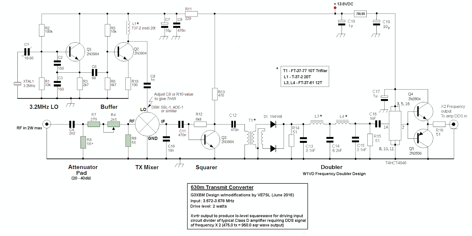
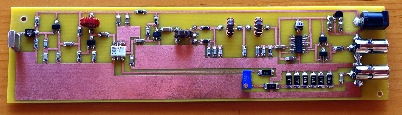
Over the past week, I've been playing with my 630m transverter summer project.
It's not the normal type of transverter that would produce a signal on 630m (~475kHz) but rather, one that will produce a signal on twice this frequency. My630m amplifier, using switching FETs, was designed and built with a 'divide-by-two' input circuit, to allow for greater frequency resolution when first constructed as a 2200m system. I really don't want to modify the transmitter and prefer just to be able to unplug my DDS and plug-in the transverter, allowing me to run WSPR, JT9 and several other digital modes when needed.
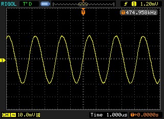
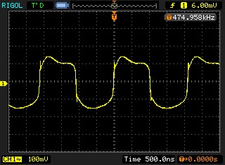
So far I've not been able to get the transverter to produce the desired low voltage 950kHz squarewave output, although I'm closer than when I began the troubleshooting.
My circuit is basically a G3XBM 630m transverter, without the FET final amplifier. Instead, the driver feeds a full-wave rectifier frequency doubler for 630m, designed and published a few years ago by Jay, W1VD. Although I can get a squarewave end result, I think harmonics creeping into the process earlier down the mixing chain are causing non-symmetry in the output.
 |
| 3.2MHz signal out of oscillator buffer stage |
 | |||
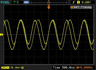
| 475 kHz signal out of mixer stage |
 |
| Signal out of 'squarer' stage |
 |
| Signal out of full-wave bridge |
 |
| Signal out of LPF |
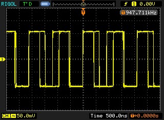 |
| Asymmetrical squarewave from 4046 output |
I've tried a 3-section LPF with a cutoff of ~600kHz between the mixer output and the next stage, trying to knock down the 'sum' frequency of 6.875MHz and any crystal harmonics but have since replaced this with a 630m diplexer at the mixer output to pass anything below 1MHz to the squarer and anything above 1.5MHz to ground. I'll keep playing with it ... until it works as it should or I have no hair left to pull out. I may also just rebuild the circuit, Manhattan-style, with normal sized parts, making it much easier to change or modify as I need. The scope grabs shown above are with the diplexer in place at the mixer output. It seems like something in the full-wave frequency doubler is amiss. I've looked at T1, the bifilar transformer several times but don't see anything odd but that's the stage where things seem to go south. Maybe it's an impedance matching-thing, something I'm yet uncomfortable with when it comes to properly matching various stages.
I also now realize that the section of transverter I have chosen will require post-mixer filtering, not shown in the schematic. Not using the last stage (FET PA) and its associated filtering, has no doubt caused more harmonics to appear in the output than anticipated. If I redesign and rebuild, I will add an LPF after the crystal oscillator as well as at the RF input port and pay more attention to post-mixer filtering.
Another route to try, rather than the W1VD doubler, may be this 4069 IC doubler or a similar 4011 doubler.
Although the project outcomes have not yet been achieved, the process has been a positive one in a couple of respects and well worth the time spent so far.
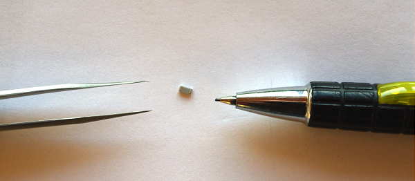
I have learned that working with the 1206-sized SMT parts is much easier than suspected and in fact, populating the board with these tiny parts was a lot of fun. The 1206-sized parts are at the 'large' end of the SMT size-spectrum ... rest assured I won't be going any smaller, at least for now.
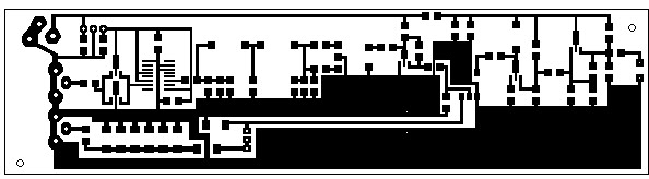
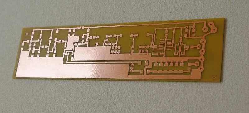
The other positive outcome was knowing that my PCB design process can work well with the narrower lines, pads and much smaller IC footprints. I still design my boards using MS Paint and have always been happy with the ease at which it works. I know many might scoff at MS Paint but it really is a very versatile little program, with a short learning curve, unlike many of the more sophisticated PCB design programs.
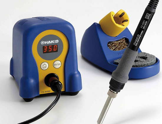
And one more positive outcome. I used the project as an excuse to purchase a new soldering station ... one that I had been lusting over for a few years as it is very SMT-friendly compared to my old Weller clunker. It also has an electrically isolated tip, unlike my Weller. The Hakko FX-888D turned out to be everything I had hoped and was no doubt part of the reason that I found the SMT process so enjoyable.
 |
| Add caption |
One Response to “Summer SMT Project”
Please support our generous sponsors who make AmateurRadio.com possible:
 Ham Radio Deluxe |
 W5SWL Electronics |
 Ham Radio Prep |
 KB3IFH QSL Cards  Hip Ham Shirts  HamRadioAuctions HamRadioAuctions Reliance Antennas Reliance Antennas Enigma Shop Enigma Shop |  morseDX  Ni4L Antennas  R&L Electronics R&L Electronics antennas.us antennas.us QRV QRV |
- Matt W1MST, Managing Editor

Steve,
Regarding your circuit, I think that the push pull output transistors will not have perfect cross over conditions unless you are using matched transistors. This can cause high current spikes due to cross conduction.
You may need to build in some dead-time to prevent this by using separate driving circuits for each transistor. This can be done with Schmitt triggers, such as 74HCT14 with RC timing circuits to introduce any desired amount of dead-time. The extra Schmitt gates can be used to help square up the pulse edges. It may also allow elimination of the 4046 circuit. PM me at w9iq at arrl dot net if you need a sketch as an example.
The high current spikes could also introduce feedback into the earlier stages. You may wish to disconnect and un-power the 4046 and the output transistors and then recheck the conditions of the earlier stages.
– Glenn W9IQ